
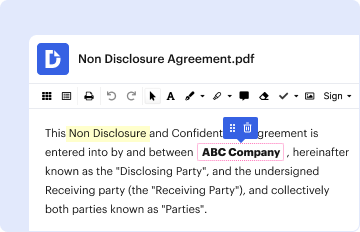

Definition and Meaning
Application Note AN-1028 is a technical document that provides comprehensive guidelines for working with BGA (Ball Grid Array) and LGA (Land Grid Array) packages. These packages are widely used in the assembly of microelectronic devices due to their high efficiency and reliability in connection. The document outlines the best practices for design, integration, and rework, ensuring optimal performance of these components in electronic setups.
Key Aspects
- BGA and LGA Packages: These are packaging technologies for mounting electronic components using arrays of solder balls or pads. They offer high-density and high-reliability connections.
- Guidelines Coverage: AN-1028 covers critical aspects such as PCB layout, solder mask openings, assembly considerations, and stencil designs.
How to Use the Application Note AN-1028
Utilizing Application Note AN-1028 involves understanding the detailed processes it outlines for handling BGA and LGA packages.
Step-by-Step Usage
- Review: Begin by thoroughly reviewing the entire document to understand the various sections and their relevance.
- PCB Layout: Follow the PCB layout instructions to ensure proper alignment and spacing for BGA/LGA components.
- Solder Mask: Implement the solder mask openings as recommended to prevent bridging and misalignment.
- Assembly Practices: Adhere to the specified assembly practices to achieve optimal reflow and adherence.
- Inspection and Rework: Utilize the inspection methods and rework procedures detailed in the application note for quality assurance.
Key Elements of the Application Note AN-1028
The application note outlines several critical components for effective implementation.
Core Components
- PCB Layout: Detailed guidelines on trace routing and pad dimensions.
- Solder Mask: Recommendations for design to prevent bridging.
- Assembly: Practices for alignment and soldering of components.
- Rework Protocols: Step-by-step rework procedures for damaged components.
Who Typically Uses the Application Note AN-1028
Professionals involved in the design and manufacturing of electronic circuits often rely on Application Note AN-1028.


Primary Users
- Electronic Engineers: They use this document to ensure proper BGA/LGA integration in circuit designs.
- Assembly Technicians: They follow the note's instructions for assembling and reworking electronic boards.
- Quality Assurance Teams: They leverage it for setting inspection standards and protocols.
Important Terms Related to Application Note AN-1028
Understanding specific terminology is crucial for effectively implementing the guidelines provided in AN-1028.
Glossary
- BGA: Ball Grid Array, a type of surface-mount packaging.
- LGA: Land Grid Array, packaging using flat connections.
- Stencil Design: The pattern for applying solder paste onto PCBs.
- Reflow Process: A method of soldering connections onto a PCB.
Legal Use of the Application Note AN-1028
The guidelines found in Application Note AN-1028 can impact compliance and quality aspects of electronic productions.
Compliance Factors
- Standards: Ensures adherence to industry standards for electronic assembly.
- Documentation: Provides formal documentation supporting quality and process integrity in manufacturing.
Examples of Using the Application Note AN-1028
Application Note AN-1028 finds utility in various real-world scenarios within the electronics manufacturing industry.
Use Cases
- Electronic Device Manufacturing: Companies manufacturing consumer electronics use AN-1028 for reliable assembly processes.
- Prototype Development: Engineers developing new electronic prototypes employ its guidelines for PCB design and testing.
- Quality Control: QA teams use it to design inspection processes and improve product reliability.
Steps to Complete the Application Note AN-1028
Though not a form that one completes, implementing the AN-1028 involves several procedural steps.
Implementation Steps
- Design Review: Begin by conducting a review of current PCB designs against the application note's guidelines.
- Process Alignment: Adjust existing manufacturing processes to incorporate recommended practices.
- Inspection Setup: Establish inspection parameters as outlined to monitor quality.
- Training: Train staff on the guidelines and procedures advised in the application note, focusing on rework and assembly techniques.
Digital vs. Paper Version
While typically distributed as a digital document, understanding the distinction between the formats can be important.
Format Attributes
- Digital Version: Easily accessible, shareable, and updates can be seamlessly integrated.
- Paper Version: Useful for on-site reference where digital access is not available, though less flexible for updates.
Software Compatibility: Application Note AN-1028
Software plays a crucial role in utilizing the guidelines from Application Note AN-1028 in practice.
Tools and Applications
- CAD Software: Used for precise PCB layout design in compliance with AN-1028.
- Solder Paste Printing Software: Assists in designing stencils according to the note's specifications.
- Reflow Simulation Software: Helps simulate and optimize reflow processes as recommended.
Application Process and Approval Time
Though not an application form, the integration of AN-1028 into workflows can be seen as a process.
Process Overview
- Initial Assessment: Conduct a gap analysis to evaluate current practices versus AN-1028 recommendations.
- Integration Plan: Develop an implementation plan addressing design, assembly, and inspection based on the application note.
- Approval and Adoption: Gain stakeholder approval and integrate AN-1028 practices into standard operating procedures for electronic assembly and quality control.