Fpga pdf 2026

Get Form
digital design using digilent fpga boards pdf Preview on Page 1

Here's how it works

01. Edit your digital design using digilent fpga boards pdf online
Type text, add images, blackout confidential details, add comments, highlights and more.
02. Sign it in a few clicks
Draw your signature, type it, upload its image, or use your mobile device as a signature pad.
03. Share your form with others
Send digital design using digilent fpga boards via email, link, or fax. You can also download it, export it or print it out.

How to use or fill out fpga pdf with our platform

Form edit decoration
9.5
Ease of Setup
DocHub User Ratings on G2
9.0
Ease of Use
DocHub User Ratings on G2
  1. Click 'Get Form' to open the fpga pdf in the editor.
  2. Begin by reviewing the introduction section, which provides an overview of digital design using FPGAs. Familiarize yourself with key concepts and components mentioned.
  3. Navigate to each example section, such as Example 1 for Switches and LEDs. Fill out any relevant fields based on your understanding of the examples provided.
  4. Utilize the block diagram editor (BDE) feature to create logic diagrams as needed for your designs. Ensure all connections are accurate before proceeding.
  5. Once you have completed filling out the necessary sections, save your work and compile it using the synthesis options available in our platform.
  6. Finally, program your FPGA board using the ExPort tool, ensuring that all settings align with your project requirements.

Engage with our platform today to streamline your FPGA design process!

be ready to get more

Complete this form in 5 minutes or less

Get form

Got questions?

We have answers to the most popular questions from our customers. If you can't find an answer to your question, please contact us.
Contact us

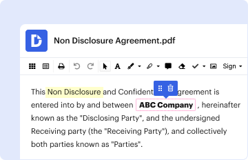
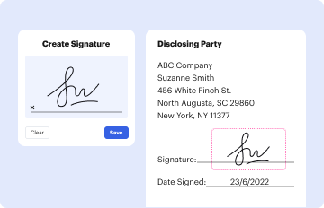
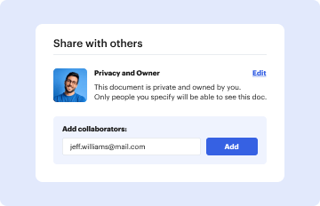
Upload your fpga book pdf to DocHub (once you’ve created an account for this). If you need to complete fields in it, use proper tools from the upper pane. For instance, add Signature Fields, assign each to a particular party, and click on Sign → Request signatures from others. Change your message for your recipients and click Send Request. You can also send your paperwork by fax or as a Signing link instead of using email (you’ll find these options by navigating to the Menu → Send)

Using a swift editing platform like DocHub, you do not require anything but a web browser and internet connection to modify your fpga digital design on the internet quickly. Upload your document or get the appropriate form in DocHub’s catalog, open our editor with a single click, and finish it electronically. To revise your forms anytime, register a free account with DocHub.

A field-programmable gate array (FPGA) is an integrated circuit designed to be configured by a customer or a designer after manufacturing \u2013 hence the term field-programmable.
The three basic types of programmable elements for an FPGA are static RAM, anti-fuses, and flash EPROM. Generic FPGA architecture. ... FPGA Configurable logic block (CLB) (courtesy of Xilinx). ... FPGA Configurable I/O block (courtesy of Xilinx). ... FPGA programmable interconnect (courtesy of Xilinx).
In general terms, FPGAs are programmable silicon chips with a collection of programmable logic blocks surrounded by Input/Output blocks that are put together through programmable interconnect resources to become any kind of digital circuit or system.

Security and compliance

At DocHub, your data security is our priority. We follow HIPAA, SOC2, GDPR, and other standards, so you can work on your documents with confidence.

Learn more
ccpa2
pci-dss
gdpr-compliance
hipaa
soc-compliance
be ready to get more

Complete this form in 5 minutes or less

Get form

People also ask

Field Programmable Gate Arrays (FPGAs) are semiconductor devices that are based around a matrix of configurable logic blocks (CLBs) connected via programmable interconnects. FPGAs can be reprogrammed to desired application or functionality requirements after manufacturing.
It is an acronym for field programmable gate array.
First and foremost, FPGAs are used to design application-specific integrated circuits (ASICs). First, you design the architecture of such a circuit. Then, you use an FPGA to build and check its prototype. Errors can be corrected.
Programming an FPGA consists of writing code, translating that program into a lower-level language as needed, and converting that program into a binary file. Then, you'll feed the program to the FPGA just like you'd do for a GPU reading a piece of software written in C++. It's as simple as that.
In general terms, FPGAs are programmable silicon chips with a collection of programmable logic blocks surrounded by Input/Output blocks that are put together through programmable interconnect resources to become any kind of digital circuit or system.

fpga tutorial pdf