
Start using our platform today for free to streamline your document editing and form completion!
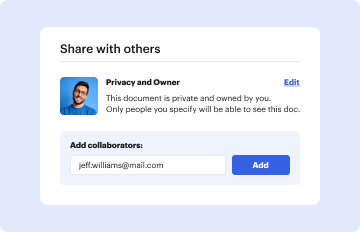
At DocHub, your data security is our priority. We follow HIPAA, SOC2, GDPR, and other standards, so you can work on your documents with confidence.
Learn more